HP Calculators custom chips around 1980
Overview
HP started designing handhelded calculators from 1968 until the end of ‘80. I buyed an HP-42S around 1993 but it has been designed near 1986.
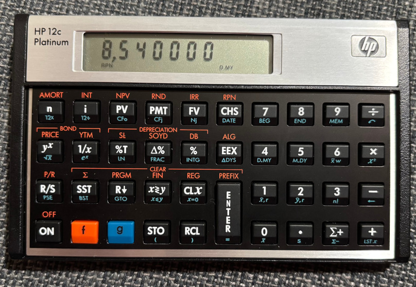
Here I want to focus on the chip design of the 10C series, a compact set of calculator with programming abilities but with full numeric display. The HP-15C was introduced in 1982, in the full 8bit computer era, the same year of the C/64. Later model will feature a more mature “Saturn” processor. I will describe here this chip at the best of my abilities, because it sheds a light on how custom architecture was done around end of 1979.
Why am I writing this article? First because I love RPN calculator, and second because to fully understand the “revolution” of 8bit microcomputer (Commodore/Apple/Atari) it is important to understand the Commodore’s competitors in the consumer calculation market.
So lets start: HP have the ability to design custom chip for its hand-helded calculator. HP have the technology to design custom RAM,ROM and so on.
The desing of this calculators includes the HP-10C, 11, 12 15 and 16. These calculators featured the “NUT” custom processor 1 labled with something like 1LH1-0304 or 1LQ9-0322.
Static RAM costs a lot. Also HP calculators used to persist state when the calculator was turned-off, so the little RAM you have, the more battery saves you get.
You have calculator designed for a specifc role, there was no a “general purpose” calculator. So there was the engineer one model (like HP-15C), and others for business men (financial one like HP-12C).
There was ever a programmer one, the HP-16C2 which had less success.
Jump start: Nibbles
In this chip you will not find 8bit bytes but 4-bit cells called nibbles. For instance a register of size 14 is composed of 14 nibbles.
The ROM microcode is stored in special 10-bit cells. So there are different size for ROM and RAM!
The processor is able to represent digit using Binary Coded Decimal (BCD) encoding which simplify display. This mode is present in MOS 6502 but very little used on this chip by Commodore/Apple!
So the HP processor ’thinks’ in decimal.
In a nibble you can store an hexdecimal digit (from $0 to $f).
I think 4bit was chosen because it offers 16 combinations, which are enough to represent a BCD number (10 combinations) and it is the smallest bit set to allow that, because with 3 bit you have only 8 combinations, which are too little.
All the main register are composed of 14 nibbles i.e. 14*4=56bit.
Also, because every ‘work’register is composed of exactly 14 nibbles, you can select one of them using just a value between 0 and 13 which easily fit in a nibble! A special Pointer register of just one nibble implements exactly this magic.
So this chip is ortagonally designed around the magic 14bit number, in a very elegant and nerd way!
Memory and Register Layout
ROM is composed of elements of 10bits Each instruction occupied 10 bits, so it is a number between $000 and 3FF. For instance the HP-12C ROM is of about $1800 elements. There are special instruction to select a ROM, up to 8 but of course it depends on the number of them provided.
-
PC Program Counter is of 16 bits / 4nibbles
-
56bit registers:
- A,B General purpose
- C is the X Register. like A,B but also interact with M to write to memory.
- D is the Y register
- E is the X register
- F is the T register
- M is a ‘scratchpad’ register for memmory access and no math operation
-
P is a special 4bit pointer register to address part of a register
S contains the status bit and it is composed of 12 niblles (48bit) DATA register is composed of 2 nibbles (8bit) to drive the address to store data of the C register. So you have at most 256x56bit of RAM, which means 1792 bytes of ’nowadays’ memory. Not all addresses write to ram: they can write to register on other specific chips. It seems the chip hhardware stack (not the RPN stack) was of size 0 or 1.
How floating point register works
Lets see how a floating point register is organized (taken from [^2] and re-designed):
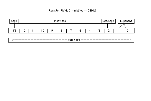
Sign: 0= positive, 9=negative.
Exponent: between 0 and 99.
Addressing
This chip has 8 selection mode, so will need at least a 3 bit to express them
| Mnemonic | meaning |
|---|---|
| p | the p register indicate the nibble to take |
| m | Select the mantissa |
| ms | mantissa +exponent |
| x | exponent |
| xs | exponent and sign |
| w | the entire register |
| wp | word up to the p register. i.e. p=3 refer to 0,1,2,3 nibbles |
| s | mantissa sign |
The chip has the ability to sum/subtract data from two registers, with a specified addressing mode, for instance subtracting mantissa(s) and so on.
The opcode description is available here
Opcode schema
1    9  8  7  6  5  4  3  2  1  0
2    <  opcode   >           opc2
3                   <field>  G  G
There are
- 7 bit opcode splitted in two areas
- A 3 bit field selector, p/m/x/w/wp/ms/xs/s
The processor use the ‘if condition holds then goto’-mode, so after an if, you have a goto instruction. The goto instruction is skipped if the condition is false.
So the ‘if’condition are in effect a if+goto instruction (20 bit) The goto bit can have only 2 valid values:
| bit | menaing |
|---|---|
| 01 | jump subroutine |
| 11 | goto to address |
The address is coded in the rest of the 8bits in a fair special way. This approach is quite different on how ARM chip works, and it is a ‘ancient’.
Conclusion and the Saturn architecture
The Saturn evolution (used in HP-42S) will extend the register to 64bit adding 2 more nibbles (going from 56 to 64 bit) increasing overall mantissa’s precision to 12 digits and extending exponent to +/-499 (collapsing sign and exponent in 3 nibbles); the overall architecture will remain more or less the same.